Semiconductors use silicon to create electronic devices. Silicon wafers are made of silicon crystals. In the manufacturing process, they are doped with gallium or boron. These impurities add donor atoms to the silicon lattice. This creates a hole that conducts current and accepts electrons from neighboring holes. The resulting material is called a P-type semiconductor. The silicon crystals are then used in integrated circuits. The thin component film is coated with a photo-resistant substance to enable the circuit pattern to be projected onto the wafer.
Silicon Wafer Manufacturing
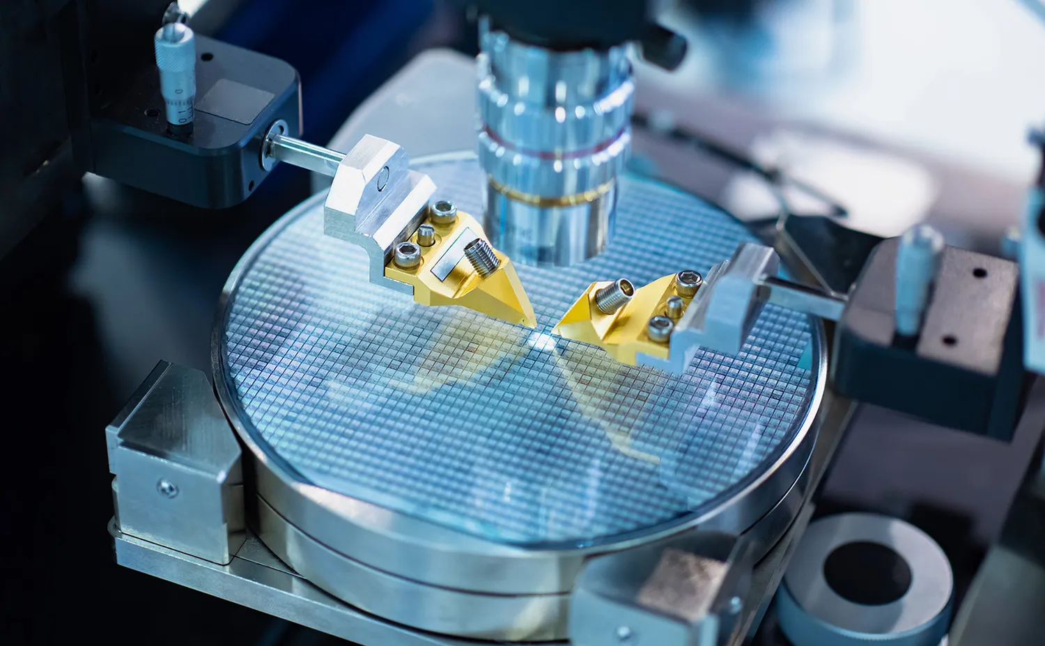
There are many steps involved in Silicon wafer manufacturing. The first step is to clean the wafers. This is important because even if the wafers are clean, small particles can remain on them and disrupt the flow of electric currents. Manufacturers must take extreme care during the cleaning process, which occurs in a clean room using specialized gear. Once the wafers have been cleaned, they must undergo a final process known as “etching.”
The next step in the Manufacturing of Silicon wafers is Crystal Pulling. In this process, a small piece of polycrystalline silicon is loaded into a Quartz crucible, where it melts under the influence of a high-purity Argon gas ambient. This melting process creates a seed of single crystal silicon that is pulled out of the molten silicon. Once the seed is pulled out of the silicon, it is then ready for the next step in the process.